The evolution of high-speed data transmission and optical sensing has reached a critical juncture where traditional discrete components no longer suffice. photonic integrated circuit components represent the pinnacle of this evolution, condensing complex optical functions—such as lasers, modulators, and detectors—onto a single semiconductor chip. By leveraging the speed of light rather than the flow of electrons, these components are redefining the boundaries of bandwidth and energy efficiency in the modern digital age.
Globally, the demand for massive data throughput in 5G/6G networks and hyperscale data centers has accelerated the adoption of integrated photonics. The ability to manipulate photons on a chip allows for an exponential increase in processing speed while drastically reducing the heat dissipation issues associated with traditional electronic circuitry. Understanding the intricacies of these components is no longer just for physicists; it is essential for engineers designing the next generation of AI hardware and quantum computing interfaces.
From a commercial perspective, the transition to integrated photonic solutions offers a path toward scalable, cost-effective manufacturing. By applying CMOS-compatible fabrication processes to optical components, the industry is moving toward a future where high-performance optical interconnects are as ubiquitous and affordable as the transistors in a standard CPU. This shift ensures that as global data traffic continues to soar, our infrastructure remains sustainable and performant.
Global Industry Context of Photonic Integration
The global semiconductor landscape is currently facing a "power wall," where the energy required to move data between electronic components exceeds the energy used for the actual computation. According to industry benchmarks aligned with ISO standards for energy efficiency, data centers now consume a significant percentage of global electricity. photonic integrated circuit components address this crisis by replacing energy-hungry copper wires with optical waveguides, slashing power consumption while increasing data rates by orders of magnitude.
Beyond data centers, the push for autonomous vehicles and real-time industrial automation requires ultra-low latency sensing. The integration of LiDAR and optical sensors directly onto chips enables these systems to process environment data in microseconds. As nations compete for leadership in the "Silicon Photonics" race, the focus has shifted from mere feasibility to mass-market scalability, ensuring that high-speed optical connectivity becomes the backbone of the global digital economy.
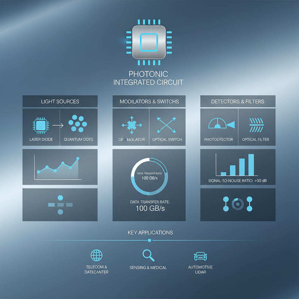
Defining Photonic Integrated Circuit Components
In the simplest terms, photonic integrated circuit components are the optical equivalent of electronic integrated circuits (ICs). While a standard IC uses transistors to switch and route electrons, a photonic IC (PIC) uses components like waveguides, modulators, and photodetectors to manipulate photons. These components are fabricated on a substrate—typically silicon, indium phosphide (InP), or lithium niobate—to create a cohesive system that can generate, route, and detect light.
The connection to modern humanitarian and industrial needs is profound. In healthcare, for instance, these components allow for the creation of "lab-on-a-chip" devices that can perform complex blood analysis or virus detection using optical spectroscopy in a fraction of the time and cost of traditional labs. This democratization of high-end diagnostic tools is only possible because PICs reduce the size of optical benches from the size of a table to the size of a fingernail.
Furthermore, these components bridge the gap between the electronic world of software and the photonic world of transmission. By integrating DACs and ADCs closely with optical modulators, the latency involved in converting electrical signals to light is minimized. This synergy is what enables the real-time synchronization required for global financial trading and large-scale scientific collaborations, such as the Square Kilometre Array (SKA) radio telescope.
Core Technical Factors for High Performance
One of the primary factors determining the efficacy of photonic integrated circuit components is Optical Loss. Every time light passes through a junction or a waveguide, a small percentage of the signal is lost. Minimizing this attenuation through precision etching and material purity is critical for maintaining signal integrity over the chip, directly affecting the maximum number of components that can be integrated into a single circuit.
Scalability and Integration Density are equally vital. The goal is to fit thousands of optical functions into a small area without causing "cross-talk," where light from one waveguide leaks into another. By utilizing advanced fabrication techniques like Silicon-on-Insulator (SOI), manufacturers can create high-confinement waveguides that allow for tighter bends and denser layouts, mirroring the scaling laws of Moore's Law for electronics.
Lastly, Thermal Stability remains a significant hurdle. Photonic components, especially ring resonators, are extremely sensitive to temperature fluctuations, which can shift the resonance frequency and cause data errors. Implementing active thermal tuning via integrated micro-heaters or using athermal materials ensures that the components operate reliably in harsh industrial environments, from freezing server rooms to high-heat automotive engines.
Real-World Applications and Use Cases
The practical deployment of photonic integrated circuit components is most evident in the realm of coherent optical communications. In transoceanic cables, these components allow for multiple wavelengths of light to be multiplexed into a single fiber, enabling terabits of data to flow between continents. This infrastructure is the silent engine powering everything from global cloud services to the streaming platforms we use daily.
In more specialized contexts, such as remote industrial zones or oil and gas exploration, integrated photonics are used for distributed acoustic sensing (DAS). By analyzing the backscatter of light in a fiber optic cable, operators can detect leaks or structural failures in pipelines over hundreds of kilometers with centimeter-level precision. This capability transforms a simple communication cable into a massive, continuous sensor, drastically reducing the need for manual inspections in dangerous environments.
Performance Efficiency of Photonic Integrated Circuit Components
Long-Term Value and Sustainability
The long-term value of adopting photonic integrated circuit components extends beyond mere speed; it is a cornerstone of environmental sustainability. By reducing the electrical power required for data transport, PICs directly lower the carbon footprint of the global internet. As AI models grow in complexity, the transition to "Optical AI" accelerators could reduce the energy consumption of training large language models by an order of magnitude.
Beyond the numbers, there is a human element of trust and reliability. In critical infrastructure, such as aerospace or medical surgery robots, the electromagnetic interference (EMI) immunity of light ensures that signals are not corrupted by external electrical noise. This provides a layer of safety and dignity in healthcare and a level of reliability in aviation that electronic systems alone cannot guarantee.
Future Trends and Material Innovations
The future of photonic integrated circuit components is moving toward "Heterogeneous Integration." Instead of relying on a single material, engineers are bonding different materials—such as III-V semiconductors for light generation and Silicon for routing—onto a single substrate. This "best-of-all-worlds" approach allows for the creation of chips that are simultaneously efficient, fast, and easy to manufacture.
Another emerging trend is the integration of photonic components with Quantum Dots and 2D materials like Graphene. These materials enable ultra-fast modulation speeds and the ability to operate at a wider range of wavelengths, which is essential for the development of a "Quantum Internet." Such a network would allow for perfectly secure communication through quantum entanglement, fundamentally changing how governments and banks handle sensitive data.
Finally, the push for "Green Photonics" is driving the development of biodegradable substrates and energy-harvesting optical components. The goal is a circular economy where the components powering our digital world do not leave a lasting scar on the physical environment, aligning digital transformation with the global ESG (Environmental, Social, and Governance) mandates.
Overcoming Implementation Challenges
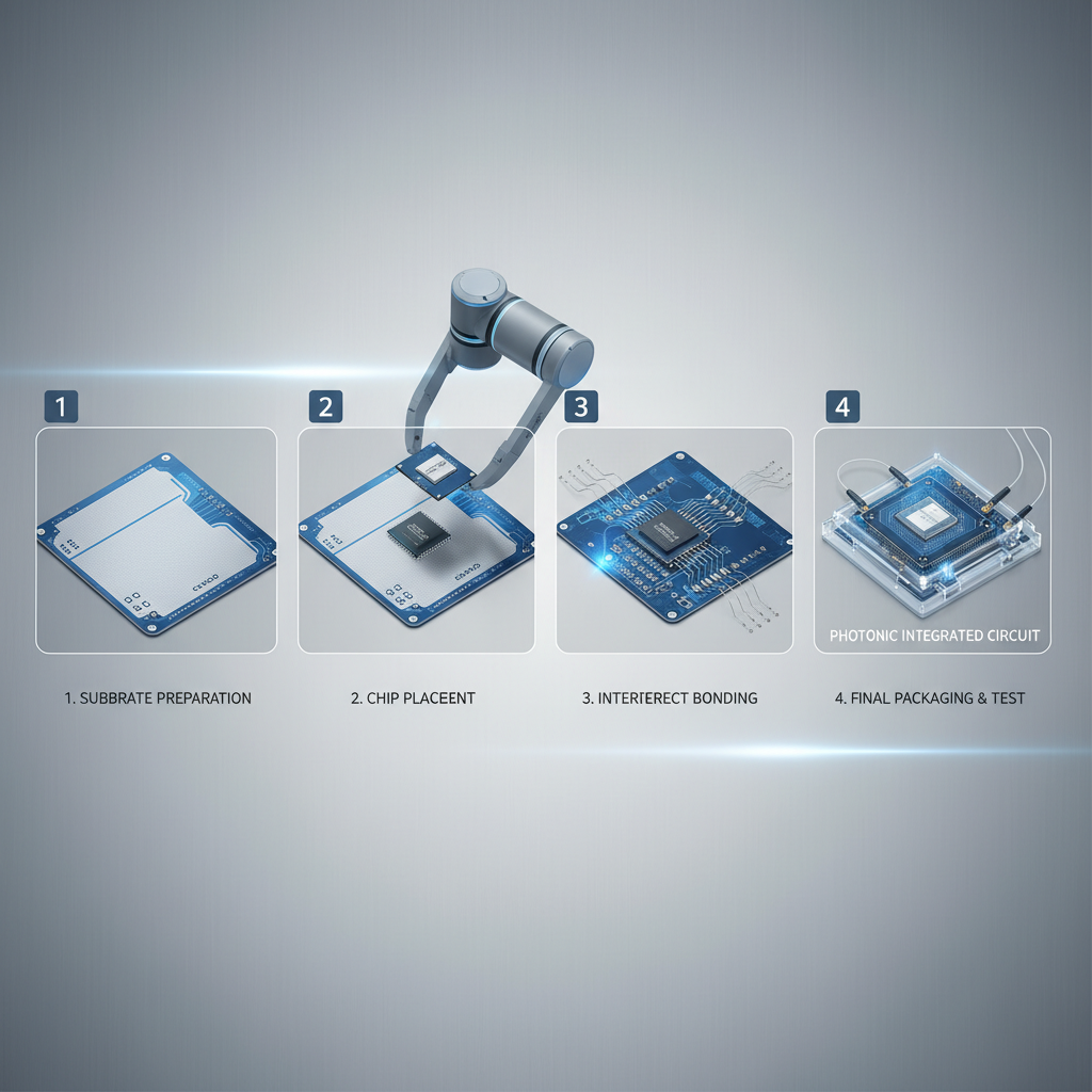
Despite the promise, implementing photonic integrated circuit components is not without hurdles. The most significant challenge is "Optical Packaging." While the chip itself is tiny, connecting it to a fiber optic cable requires sub-micron alignment precision. A misalignment of just 500 nanometers can lead to massive signal loss, making the assembly process expensive and time-consuming.
To solve this, the industry is moving toward automated "flip-chip" bonding and grating couplers that allow light to be coupled vertically rather than horizontally. By utilizing machine-learning-driven alignment systems, manufacturers are reducing the cost of packaging and increasing the yield of usable chips, moving PICs closer to the price points of standard electronics.
Another limitation is the lack of standardized design tools. Unlike the mature EDA (Electronic Design Automation) tools for transistors, photonic design tools are still evolving. The solution lies in the creation of open-source photonic PDKs (Process Design Kits), allowing engineers worldwide to collaborate and standardize the "building blocks" of photonic circuits, thereby accelerating the time-to-market for new innovations.
Analysis of Photonic Integrated Circuit Components Fabrication and Performance
| Material Platform |
Integration Complexity |
Energy Efficiency |
Market Adoption |
| Silicon Photonics (SiPh) |
Low (CMOS compatible) |
High (8/10) |
Very High |
| Indium Phosphide (InP) |
Medium |
Medium (6/10) |
High (Lasers) |
| Lithium Niobate (LiNbO3) |
High |
High (9/10) |
Medium (Niche) |
| Silicon Nitride (Si3N4) |
Low |
High (7/10) |
Growing |
| GaAs-based PICs |
Medium |
Medium (7/10) |
Moderate |
| Hybrid Polymer-Si |
Medium |
Low (5/10) |
Experimental |
FAQS
The primary advantage lies in bandwidth and energy efficiency. While electronic circuits are limited by resistance and capacitance (RC delays), photonic components use light, which allows for significantly higher data transfer rates with far less heat generation. This makes them ideal for long-distance communication and high-performance computing where energy costs are a major concern.
Many photonic ICs use silicon photonics, which leverages existing CMOS fabrication plants. This means they can be made using the same lithography and etching tools as standard CPUs. However, because light requires different material properties for generation (like InP for lasers), hybrid integration is often used to bond non-silicon materials onto the silicon chip.
Currently, they are mostly used in infrastructure (data centers, telecom). However, as costs drop due to scalable manufacturing, we expect to see them in consumer devices, such as ultra-fast wireless routers or advanced medical wearables, where high-sensitivity optical sensing is required in a compact form factor.
Signal loss typically occurs due to scattering at the waveguide walls (surface roughness), absorption by the material, and bending losses where the light "leaks" out of a curve that is too sharp. Precision nanofabrication and the use of high-refractive-index contrast materials are the primary solutions to these issues.
Yes, they are specifically designed to be. In fact, photonic ICs act as the bridge between the fiber optic cable and the electronic processor. They convert the light signals from the fiber into electrical data that a computer can understand, and vice versa, which is why they are critical for the "last inch" of data transmission.
Because light wavelengths are so small, even a tiny change in temperature can change the refractive index of the material, shifting the device's operating frequency. Thermal tuning involves using micro-heaters to precisely maintain the temperature of a component (like a ring resonator), ensuring it stays "in tune" with the signal it is processing.
Conclusion
The transition toward photonic integrated circuit components represents one of the most significant leaps in semiconductor history. By merging the computational power of electronics with the transmission speed of photonics, we are overcoming the physical limitations of copper and electricity. From reducing the carbon footprint of the global internet to enabling the next generation of medical diagnostics and AI, the value of these components lies in their ability to deliver unprecedented performance without compromising sustainability.
Looking forward, the democratization of photonic design tools and the mastery of heterogeneous integration will accelerate the adoption of this technology across all industrial sectors. For companies and engineers, the strategy should be to embrace hybrid architectures that combine the strengths of both electrons and photons. As we stand on the precipice of the quantum era, integrated photonics will undoubtedly be the catalyst that transforms these theoretical possibilities into tangible commercial realities. Visit our website for more insights: www.ckxic.com