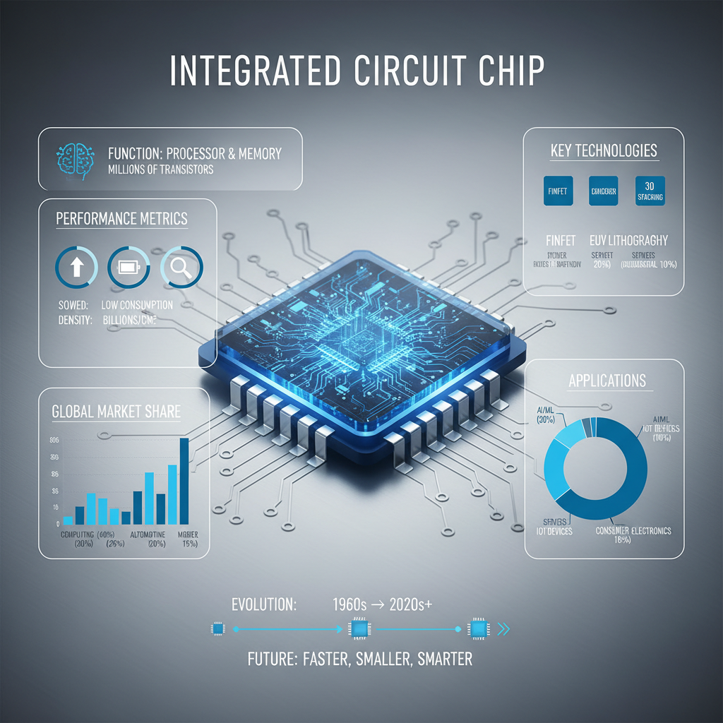
The modern technological landscape is fundamentally underpinned by the integrated circuit chip, a marvel of engineering that has shrunk entire rooms of vacuum tubes into microscopic silicon wafers. From the smartphone in your pocket to the advanced medical imaging systems in hospitals, these components facilitate the rapid processing of data and the precise control of electronic signals. Understanding the nuances of these semiconductors is no longer just for engineers; it is essential for any business navigating the digital transformation of the 21st century.
Globally, the demand for highly efficient integrated circuit chip solutions has surged as industries shift toward automation, Artificial Intelligence, and the Internet of Things (IoT). According to recent industry trends and ISO standards for electronic components, the drive toward miniaturization and lower power consumption is accelerating. However, this growth comes with challenges, including supply chain volatility and the increasing complexity of chip architecture, which requires a deeper understanding of component selection to ensure system reliability.
By mastering the application of various semiconductor types—such as ADC/DACs for signal conversion or Microcontrollers for system logic—companies can significantly reduce their time-to-market and improve product durability. This guide explores the intricate world of the integrated circuit chip, breaking down complex parameters into actionable insights to help you optimize your electronic designs for maximum performance and cost-efficiency.
Understanding the Fundamentals of the Integrated Circuit Chip
At its simplest level, an integrated circuit chip is a set of electronic circuits on one small flat piece of semiconductor material, usually silicon. Instead of connecting separate transistors, resistors, and capacitors with wires, these components are fabricated directly into the substrate. This integration allows for an unprecedented increase in speed and a dramatic decrease in the physical footprint of electronic devices.
This technological leap has enabled the creation of everything from simple timers to complex processors capable of billions of operations per second. In the context of modern manufacturing, the ability to integrate diverse functions—such as memory, logic, and analog signal processing—onto a single die has revolutionized how we approach product design, making devices more portable and energy-efficient than ever before.
Key Factors Influencing Semiconductor Performance
When evaluating an integrated circuit chip, scalability is one of the most critical factors. As we move toward smaller nanometer nodes, the ability to pack more transistors into a smaller area increases processing power. However, this also introduces challenges like quantum tunneling and heat dissipation, which engineers must mitigate through innovative materials and packaging techniques.
Thermal stability and durability are equally paramount, especially in industrial environments. A chip designed for a consumer toy cannot withstand the extreme temperatures of an automotive engine control unit or the high-radiation environment of aerospace equipment. Therefore, the choice of substrate and the quality of the encapsulation process directly impact the long-term reliability of the final product.
Finally, cost-efficiency remains a driving force in the semiconductor industry. Balancing the performance of a high-end SoC (System on Chip) against the cost of production requires a strategic approach to yield management. By optimizing the design for manufacturability, companies can ensure that their integrated circuit chip solutions remain competitive without sacrificing the rigorous quality standards required by global markets.
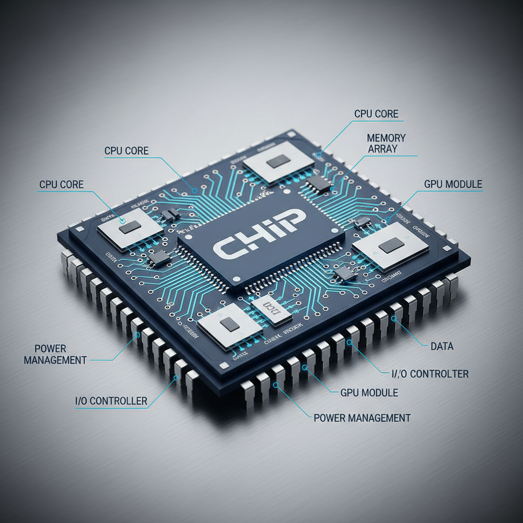
Core Components and Their Industrial Roles
The ecosystem of the integrated circuit chip is divided into several specialized categories. For instance, ADC/DACs are the bridges between the analog world and digital processing, while Amplifiers ensure that weak signals are boosted enough to be readable by subsequent stages of the circuit.
More complex roles are filled by Microcontrollers and Logic Devices, which act as the "brains" of the operation. These components manage data flow, execute programmed instructions, and interface with external sensors, making them indispensable for any integrated circuit chip application involving automation or intelligent decision-making.
Supporting these are Memory chips, Interface ICs, and Clocks & Timers, which provide the necessary infrastructure for data storage, communication, and synchronization. Without these specialized elements, an integrated circuit chip would be unable to coordinate the complex timing required for high-speed data transmission in modern telecommunications.
Global Applications and Strategic Use Cases
The versatility of the integrated circuit chip is evident in its widespread adoption across diverse sectors. In the medical field, highly precise sensors and ADC chips enable real-time patient monitoring and the development of non-invasive diagnostic tools. In remote industrial zones, ruggedized interface ICs allow for the monitoring of pipeline integrity and power grid stability under harsh weather conditions.
Furthermore, in the realm of green energy, power management ICs are crucial for optimizing the efficiency of solar inverters and electric vehicle batteries. By precisely controlling the flow of current, these chips reduce energy waste and extend the lifecycle of expensive battery packs, proving that the integrated circuit chip is a cornerstone of sustainable development and global carbon reduction efforts.
Comparative Performance of IC Architectures
Tangible Advantages and Long-Term Value
Integrating a high-quality integrated circuit chip into your product design offers immediate logical benefits, primarily in the form of reduced power consumption and increased reliability. By replacing discrete components with an integrated solution, manufacturers can eliminate numerous solder points—the most common failure points in electronics—thereby increasing the overall mean time between failures (MTBF).
Beyond the technical specs, there is an emotional value rooted in trust and safety. When a medical device or an automotive braking system relies on a certified, high-performance integrated circuit chip, it provides peace of mind to the end-user. This reliability fosters brand loyalty and establishes a reputation for excellence, turning technical superiority into a sustainable commercial advantage.
Future Trends in Chip Innovation
The future of the integrated circuit chip is leaning heavily toward the adoption of Wide Bandgap (WBG) materials like Gallium Nitride (GaN) and Silicon Carbide (SiC). These materials allow chips to operate at much higher voltages and temperatures than traditional silicon, which is revolutionary for the next generation of fast chargers and high-power industrial converters.
Additionally, we are seeing a shift toward "Chiplet" architecture, where instead of one massive die, several smaller, specialized chips are interconnected in a single package. This approach improves yields and allows for a mix-and-match strategy where different process nodes can be used for different functions within the same integrated circuit chip module.
Digital transformation and the rise of Edge AI are also pushing the boundaries of on-chip processing. By moving the AI inference from the cloud directly onto the integrated circuit chip at the edge, we can achieve near-instantaneous response times and enhanced data privacy, paving the way for truly autonomous systems.
Overcoming Current Challenges in Chip Implementation
One of the most pressing challenges in the industry is the "dark silicon" problem, where a significant portion of the integrated circuit chip must remain powered off to prevent overheating. To overcome this, architects are moving toward domain-specific accelerators—specialized circuits that perform one task extremely efficiently, rather than using a general-purpose processor for everything.
Supply chain resilience has also become a top priority. The industry is moving away from a single-source dependency toward a more diversified fabrication strategy. By designing integrated circuit chip layouts that are portable across different foundries, companies can protect themselves from regional disruptions and geopolitical instability.
Finally, the integration of advanced testing and validation protocols is essential to combat the rising complexity of chip designs. Implementing "Design for Test" (DFT) methodologies ensures that defects are caught early in the production cycle, reducing waste and ensuring that every integrated circuit chip shipped meets the strict performance criteria of the end application.
Analysis of Integrated Circuit Chip Implementation Strategies
|
Strategy Type
|
Complexity Level
|
Performance Gain
|
Cost Impact
|
| Discrete to IC Migration |
Low |
Moderate |
Significant Reduction |
| Chiplet Integration |
High |
Very High |
Moderate Increase |
| GaN/SiC Material Shift |
Medium |
High (Efficiency) |
Initial Increase |
| Edge AI Implementation |
High |
Ultra-Low Latency |
Moderate Increase |
| DFT Methodology |
Medium |
Consistency Gain |
Long-term Saving |
| Low-Power Optimization |
Medium |
Extended Battery Life |
Neutral |
FAQS
A discrete circuit uses separate components (individual transistors, resistors, capacitors) connected by wires on a PCB. In contrast, an integrated circuit chip integrates all these components onto a single semiconductor substrate. This results in a much smaller size, lower power consumption, and generally higher speed and reliability due to the reduction of external connections.
You should look for "Industrial Grade" or "Automotive Grade" specifications. These chips are tested for wider temperature ranges (e.g., -40°C to +125°C) and often use advanced packaging materials to prevent thermal expansion cracks. Always verify the thermal resistance (Theta-JA) in the datasheet to ensure your heat sinking strategy is adequate.
It depends on the type. Standard ASICs (Application-Specific Integrated Circuits) are hard-wired and cannot be changed. However, MCUs (Microcontrollers) and FPGAs (Field Programmable Gate Arrays) are designed to be programmable. FPGAs, in particular, allow the hardware logic itself to be redefined after the chip has been placed in the system.
The real world is analog (sound, light, temperature), but computers are digital. ADC (Analog-to-Digital Converter) chips translate these real-world signals into binary data for processing. DAC (Digital-to-Analog Converter) chips do the opposite, converting digital data back into analog signals to drive speakers, motors, or displays.
Dark silicon refers to the portion of an integrated circuit chip that cannot be powered on at any given time because the heat generated would exceed the chip's cooling capacity. Designers solve this by creating highly specialized accelerators that only turn on when needed, reducing the average power density while maintaining high peak performance.
Initially, yes, because the fabrication processes for Gallium Nitride and Silicon Carbide are more complex than traditional silicon. However, the long-term value is high; they allow for smaller heat sinks and significantly higher energy efficiency, which reduces the total system cost and increases the product's market value.
Conclusion
The integrated circuit chip remains the most critical building block of the digital age, evolving from simple logic gates to complex systems-on-chip that drive everything from AI to sustainable energy. By understanding the balance between scalability, thermal stability, and component specialization—ranging from ADC/DACs to Microcontrollers—engineers and businesses can build products that are not only powerful but also reliable and cost-effective.
As we look toward a future of Chiplets, Edge AI, and Wide Bandgap materials, the importance of selecting the right semiconductor partner becomes paramount. Embracing these innovations will allow companies to overcome current hardware limitations and lead the next wave of technological breakthroughs. For high-quality, reliable components and expert guidance on your next project, visit our website: www.ckxic.com