The modern digital landscape is built upon the invisible architecture of the integrated circuit device, a marvel of engineering that consolidates millions of electronic components onto a single semiconductor wafer. From the smartphone in your pocket to the sophisticated control systems in industrial robotics, these devices enable the high-speed processing and memory storage that define the 21st century. Understanding the intricacies of these components is no longer just for engineers; it is essential for any business looking to navigate the complexities of the global electronics supply chain.
Globally, the demand for a high-performance integrated circuit device has surged as we transition toward an era of ubiquitous computing and the Internet of Things (IoT). This surge is driven by the need for smaller form factors, lower power consumption, and unprecedented computational density. As industries shift toward automation and AI-driven analytics, the role of the semiconductor has evolved from a simple switch to the cognitive core of autonomous systems, making it the most critical commodity in the modern geopolitical economy.
However, this reliance brings significant challenges, including supply chain volatility and the physical limits of silicon-based fabrication. By exploring the fundamental principles, applications, and future trajectories of the integrated circuit device, stakeholders can better anticipate technological pivots and optimize their hardware selection. Whether it is implementing precise ADC/DAC converters or deploying high-efficiency power transistors, the strategic choice of ICs determines the reliability, scalability, and longevity of the final product.
Global Relevance of the Integrated Circuit Device
The strategic importance of the integrated circuit device is mirrored in the economic data of the last decade. According to industry reports and global trade statistics, semiconductors now underpin nearly every sector of the GDP in developed nations, from automotive manufacturing to healthcare. The global shift toward "Industry 4.0" has transformed these chips from optional components into the foundational infrastructure of global trade, where a shortage in a single fabrication plant can stall entire automotive assembly lines across continents.
This global dependence highlights a critical vulnerability: the concentration of high-end fabrication. As we move toward more complex nodes, the precision required to manufacture an integrated circuit device has reached atomic scales. This has led to a global race for "silicon sovereignty," where nations are investing billions to secure their own supply chains, ensuring that the digital pulse of their infrastructure remains uninterrupted by geopolitical instability.
Defining the Modern Integrated Circuit Device
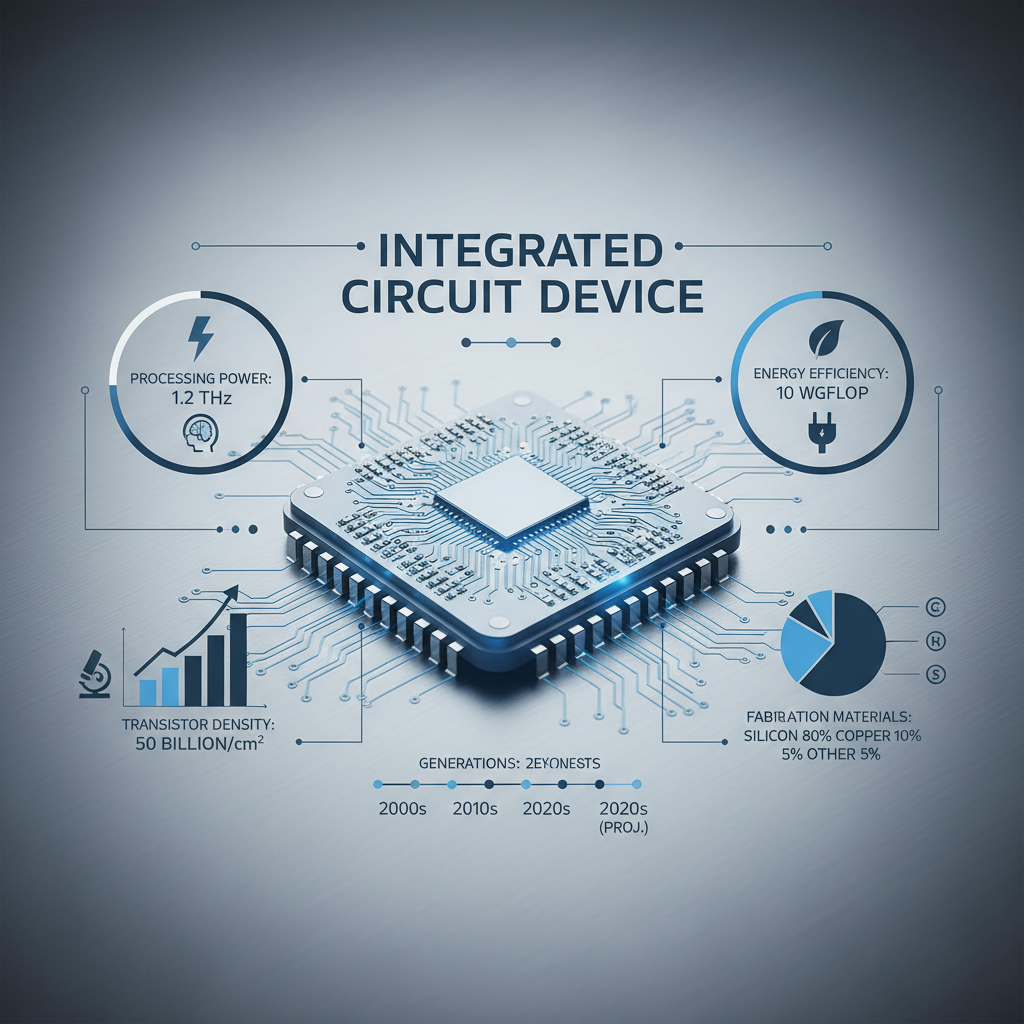
In the simplest terms, an integrated circuit device (IC) is a set of electronic circuits on one small flat piece of semiconductor material, usually silicon. Unlike discrete circuits, where resistors, capacitors, and transistors are connected by wires on a board, the IC integrates all these functions into a single monolithic block. This miniaturization allows for an exponential increase in speed and a drastic reduction in power consumption, which is why modern computers can fit in a pocket rather than filling a room.
Beyond the technical definition, the IC is the bridge between the physical and digital worlds. For instance, in humanitarian efforts, low-cost ICs enable the deployment of portable water filtration sensors and solar-powered medical diagnostic tools in remote areas. By integrating complex logic into a cheap, durable package, the integrated circuit device democratizes access to technology, allowing life-saving innovations to be scaled and distributed globally at a fraction of the cost of legacy systems.
Modern ICs are generally categorized into analog, digital, and mixed-signal devices. Analog ICs, such as Amplifiers and Sensors, handle continuous signals; digital ICs, like Microcontrollers and Logic Devices, process binary data; and mixed-signal ICs, including ADC/DAC converters, bridge the two. This synergy allows a device to sense a temperature change in the environment, convert that analog voltage into a digital number, and then trigger a logic-based response—all within a few square millimeters of silicon.
Core Components and Technical Factors
The efficacy of an integrated circuit device is primarily determined by its thermal management and signal integrity. As transistors shrink, the heat generated per unit area increases, making thermal dissipation a critical design factor. Advanced packaging techniques, such as Flip-Chip or 3D-IC stacking, are employed to ensure that high-performance chips do not throttle their clock speeds due to overheating, thereby maintaining consistent operational stability.
Scalability and power efficiency are the twin pillars of modern integrated circuit device design. By utilizing FinFET technology and Gate-All-Around (GAA) transistors, engineers can reduce leakage current and lower the operating voltage. This is particularly vital for battery-operated devices and remote industrial sensors, where extending the operational life of a device from two years to ten years can save millions in maintenance costs.
Furthermore, the reliability of an integrated circuit device in harsh environments depends on the materials used in its fabrication. For aerospace or automotive applications, "automotive-grade" ICs are used, which are tested to withstand extreme temperature swings and high vibration. The integration of wide-bandgap materials like Gallium Nitride (GaN) or Silicon Carbide (SiC) is now replacing traditional silicon in power-heavy applications to increase durability and efficiency.
Performance Metrics and Efficiency Analysis
Evaluating an integrated circuit device requires a multi-dimensional approach, looking beyond raw clock speed. Key performance indicators (KPIs) include the power-delay product (PDP), which measures the energy consumed per switching operation, and the signal-to-noise ratio (SNR) for analog components. In the realm of Interface ICs and Memory, latency and throughput determine how quickly data can move between the processing core and the peripheral devices.
To optimize these metrics, designers often employ a trade-off analysis between cost, area, and power. For a mass-market consumer product, a slight increase in power consumption might be acceptable if it significantly reduces the die size and thus the unit cost. Conversely, for medical implants or space-grade hardware, the priority shifts entirely toward reliability and ultra-low power consumption, regardless of the manufacturing cost.
Efficiency Comparison of Integrated Circuit Device Architectures
Real-World Global Applications
The application of an integrated circuit device spans every imaginable sector. In the automotive industry, the transition to Electric Vehicles (EVs) has created a massive demand for specialized power ICs and battery management systems that can handle high voltages while maintaining millisecond-level precision. In the medical field, miniaturized ICs are the core of wearable health monitors that track glucose levels or heart rhythms in real-time, transmitting data to doctors via low-energy wireless protocols.
In remote industrial zones, such as oil rigs or deep-sea mining operations, ruggedized integrated circuit device modules are used to monitor structural integrity and environmental hazards. These devices must operate without human intervention for years, utilizing ultra-low-power timers and high-reliability memory to ensure that critical alerts are delivered even in the most hostile conditions. This blend of reliability and intelligence is what enables the scaling of global infrastructure in unreachable terrains.
Long-Term Value and Innovation Benefits
Investing in the right integrated circuit device provides value far beyond the initial purchase price. The primary long-term benefit is the dramatic reduction in Total Cost of Ownership (TCO). By utilizing highly integrated modules—such as combining a microcontroller, clock, and interface IC into a single system-on-chip (SoC)—companies can reduce their Bill of Materials (BOM), simplify their PCB layouts, and decrease the failure rate associated with multiple solder joints and interconnects.
From a sustainability perspective, the evolution of IC design is a key driver in the global effort to reduce carbon footprints. More efficient chips mean less energy wasted as heat, which in turn reduces the cooling requirements for massive data centers. When an integrated circuit device is optimized for "green computing," it doesn't just save money; it contributes to a more sustainable technological ecosystem by lowering the aggregate energy demand of the digital economy.
Moreover, the psychological impact of reliable hardware cannot be overstated. In mission-critical systems—such as aviation flight controls or nuclear power plant monitoring—the trust placed in the semiconductor is absolute. The innovation in error-correcting code (ECC) memory and redundant logic circuits ensures that these devices can detect and fix their own faults, providing a level of safety and dignity to human operators who rely on these systems for survival.
Future Trends in Semiconductor Evolution
The future of the integrated circuit device is moving toward "More than Moore," a philosophy that looks beyond simply shrinking transistors. We are seeing the rise of Heterogeneous Integration, where different types of chips (analog, digital, and optical) are combined into a single package using advanced chiplet technology. This allows for the creation of specialized accelerators for AI and machine learning that are far more efficient than general-purpose CPUs.
Another groundbreaking trend is the integration of Neuromorphic Computing, where the integrated circuit device is designed to mimic the neural structure of the human brain. By processing information in parallel and using "spiking" neural networks, these devices could potentially perform complex pattern recognition tasks using a fraction of the energy required by current GPUs, paving the way for truly autonomous edge AI.
Finally, the shift toward sustainable materials is becoming mandatory. The industry is exploring biodegradable substrates and lead-free fabrication processes to mitigate the environmental impact of electronic waste. As we move toward a circular economy, the design of the integrated circuit device will be influenced not only by how it performs during its life but also by how easily it can be recycled at the end of its cycle.
Comparison of Emerging Integrated Circuit Device Technologies
| Technology Path |
Primary Benefit |
Target Application |
Adoption Maturity |
| Chiplet Architecture |
Higher Yield & Modular Design |
High-Performance Computing |
High |
| GaN/SiC Power ICs |
Ultra-High Efficiency |
EV Charging & Power Grids |
Medium-High |
| Neuromorphic ICs |
Brain-like Processing |
Edge AI & Robotics |
Low-Medium |
| Optical ICs |
Light-speed Data Transfer |
Data Center Interconnects |
Medium |
| 3D-IC Stacking |
Extreme Density |
Mobile SoC & HBM Memory |
High |
| Bio-compatible ICs |
In-vivo Integration |
Neural Implants |
Low |
FAQS
A discrete component is a single electronic unit (like one resistor or one transistor) that performs a specific function. An integrated circuit device, however, combines thousands or millions of these components onto a single semiconductor wafer. This integration reduces the physical size of the circuit, lowers power consumption, and increases operating speed, making it possible to create complex devices like microprocessors that would be impossible to build using discrete parts.
The choice affects longevity through thermal efficiency and material durability. Higher-quality ICs with better thermal management prevent degradation caused by heat stress. Furthermore, selecting "industrial-grade" or "automotive-grade" devices ensures the chip can handle extreme temperatures and vibrations without failing, significantly extending the operational lifespan of the end product compared to standard consumer-grade components.
While silicon is the most common material due to its abundance and stable oxide layer, it is not the only one. Depending on the application, materials like Gallium Arsenide (GaAs) are used for high-frequency radio applications, and Gallium Nitride (GaN) or Silicon Carbide (SiC) are used for high-power and high-temperature applications where traditional silicon would fail or be inefficient.
A mixed-signal IC is a device that contains both analog and digital circuits on the same chip. The most common examples are ADC (Analog-to-Digital Converters) and DAC (Digital-to-Analog Converters). These are essential because the real world is analog (sound, light, temperature), but computers process data digitally. Mixed-signal devices allow the system to bridge these two domains seamlessly.
Companies can mitigate risks by adopting a "multi-sourcing" strategy, where they design their hardware to be compatible with equivalent integrated circuit devices from different manufacturers. Additionally, moving toward more standardized components and maintaining strategic buffers of critical ICs can protect production lines from sudden market volatility or geopolitical disruptions.
Yes, as transistors approach the size of a few atoms, "quantum tunneling" occurs, where electrons leak through barriers, causing errors and heat. To overcome this, the industry is moving toward 3D-IC stacking (building upward) and exploring new materials and architectures, like GAAFETs and optical computing, to continue improving performance without relying solely on shrinking the size.
Conclusion
The integrated circuit device stands as the most influential invention of the modern era, enabling everything from the simplest timer to the most complex artificial intelligence. By integrating diverse functions—such as sensing, processing, and memory—into a single semiconductor package, ICs have fundamentally altered the cost-structure and capabilities of global technology. From the precision of ADC/DAC converters to the raw power of microcontrollers, these devices are the essential building blocks of sustainable, efficient, and scalable industrial growth.
Looking forward, the trajectory of semiconductor evolution points toward a future of heterogeneous integration and neuromorphic design, where the boundary between hardware and biological efficiency begins to blur. For engineers and procurement specialists, the key to success lies in selecting components that balance current performance needs with future-proof scalability. As we navigate the transition toward a greener, more automated world, the strategic implementation of high-performance ICs will remain the primary differentiator for innovative companies. Visit our website: www.ckxic.com